If you’ve ever worked in hardware design and/or verification, you know that discovering a power problem late in the design is a nightmare. You’ve already synthesized, placed, and routed the chip and now someone tells you a module is drawing twice the expected power. At that point, fixing it means going all the way back to the beginning. VCD2Activity is about preventing exactly that.
1. Why Does Power Matter and Why Is It So Hard To Catch Early?
Let’s start with a real example [1]. In 2022, Qualcomm’s Snapdragon 8 Gen 1 processor landed in flagship smartphones from Samsung, Xiaomi, and others. The chip was functionally correct with all its logic working as intended. The problem was that under sustained load, it overheated. Independent benchmarks showed it drawing excessive power, forcing phones to throttle performance just to avoid burning up. Qualcomm had to release a mid-cycle replacement chip, the Snapdragon 8+ Gen 1, just to fix the power behavior. That’s an enormous cost in time, money, and brand reputation.
Power consumption matters for three practical reasons:
- Heat: Energy that doesn’t become useful work becomes heat. Too much heat means thermal throttling, permanent damage, or complete failure.
- Cost: A chip that runs hot needs bigger heat sinks, specialized packaging, and larger fans; all of which add up in the bill of materials.
- Battery life: For mobile and IoT devices, every milliwatt counts. Poor power estimation leads to products that die halfway through the day.
The frustrating thing is that catching power problems late is also expensive to fix. This is why power estimation should happen as early as possible, ideally concurrently with the chip implementation and verification.
2. Power Estimation Levels – What Are They?
In a typical chip design flow, a design goes through several stages before a physical chip is manufactured. The process looks roughly like this:
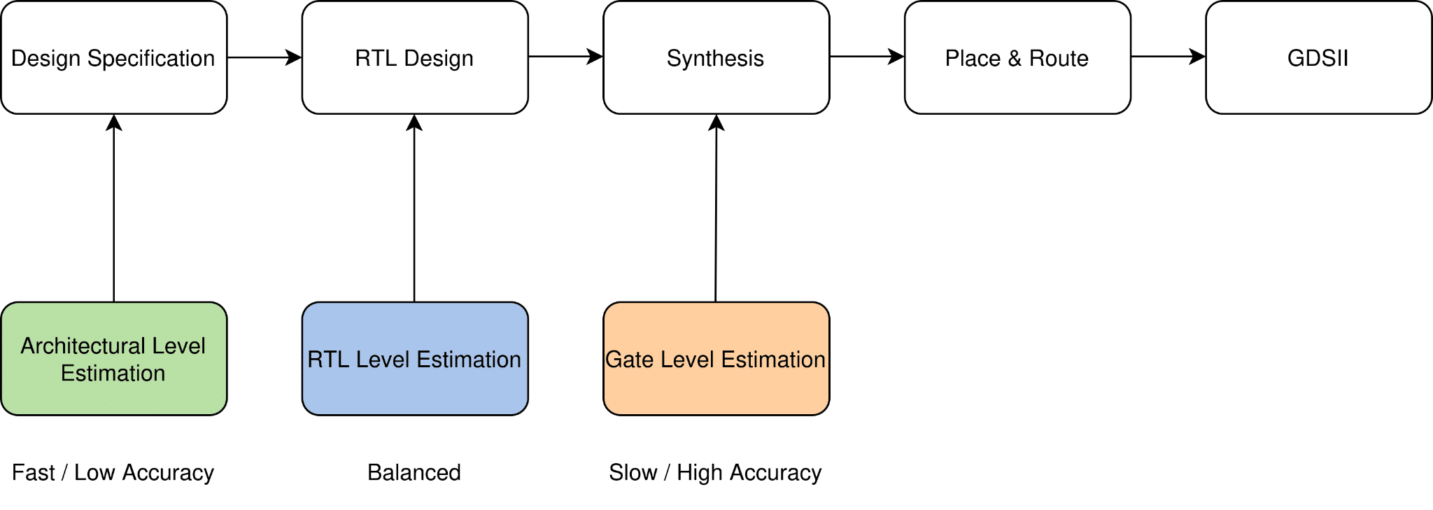
Fig 1. The hardware design flow
Power estimation can happen at three points in this flow:
Architectural Level
At this stage, there’s no actual hardware yet, just a specification document. Engineers estimate power based on experience from previous similar chips. It’s fast, but it’s essentially an educated guess. Decisions made at this level carry the biggest long-term impact, since they shape the entire architecture.
RTL Level
Once you write the hardware in an HDL like Verilog or SystemVerilog, you can simulate it. Teams already run simulations for functional verification anyway, so you can extract power insights at essentially no extra cost. This is the sweet spot: accurate enough to be meaningful, cheap enough to run early and often. VCD2Activity lives here.
Gate Level
Synthesis maps the design to actual physical logic gates. Power analysis at this stage is the most accurate because it calculates the exact capacitance of every wire and gate. The catch? Synthesis can take hours or days, and running simulations at gate level can take even longer, sometimes weeks for complex designs.
The RTL gap: Engineers run RTL simulations constantly, and every simulation automatically produces a file full of toggle activity data. But there’s no easy, free way to turn that data into useful power insights. That’s the problem VCD2Activity solves by estimating toggle activity.
3. What Is a VCD File and Why Do We Care?
A VCD (Value Change Dump) [2] file is typically produced after simulation. The VCD format is the only standardized format and there are converters from virtually any format to VCD, so this project was built around it. It records every single time any signal in the design changes its value, along with the exact timestamp. Think of it as a timestamped event log for every wire and register in your circuit.
The connection to power is direct, as the power formula is the following:
PTotal = PStatic + PDynamic + PShort-circuit
Fig 2. The power formula
Dynamic power consumption follows this formula:
PDynamic = α · Cload · Vdd2 · f
Fig 3. The dynamic power formula
The key insight is that α (the activity factor), how often signals toggle, is the only component of this formula that reflects actual design behavior in simulation. Cload (wire capacitance) and Vdd (supply voltage) come from the physical manufacturing process and aren’t known until after place and route. While f (clock frequency) is a known design specification, it functions as a global constant for the system or a certain domain and does not reveal localized power inefficiencies. But α is right there in every VCD file, if you know how to extract it.
4. Preliminary Research
Before settling on the RTL-level approach, some time was spent exploring how power analysis is performed at the gate level in practice, to better understand what VCD2Activity would eventually be complementing and how difficult it would have been to implement a gate-level tool. The tools used were open-source EDA tools, which provided a transparent look at standard power estimation workflows.
Yosys [3] is an open-source synthesis framework that takes RTL code written in Verilog and maps it to a gate-level netlist targeting a specific technology library. Running synthesis through Yosys gave a clearer picture of what happens between the RTL stage and the physical implementation. It also shows how abstract hardware descriptions become networks of actual logic gates, and how much the structure of the design changes in that process.
OpenROAD [4] is an open-source tool that takes a synthesized netlist and performs place and route, determining the physical location of every gate on the silicon die and drawing the metal connections between them. Going through this flow made it concrete how late in the process physical parameters like wire capacitance become available, and why waiting until gate level to estimate power is so expensive in terms of time.
The SkyWater 130nm PDK (Process Design Kit) [5] was used as the target technology for these experiments. A PDK defines the electrical and physical characteristics of every cell available in a manufacturing process, like transistor sizes, wire resistance, capacitance per unit length, and more. Working with it illustrated exactly which parameters feed into power calculations at the gate level and why none of them are available at the RTL stage, reinforcing the motivation for building a tool that works directly from simulation output instead.
5. The VCD2Activity Architecture
The first big design decision was performance. Python seemed like the obvious language, it’s fast to develop in and has great visualization libraries. But after testing on realistic VCD files, the problem became clear: Python’s interpreted nature makes it slow at sequential file parsing. Industrial VCD files can reach hundreds of gigabytes. A pure-Python parser just can’t keep up.
The solution was a hybrid architecture:
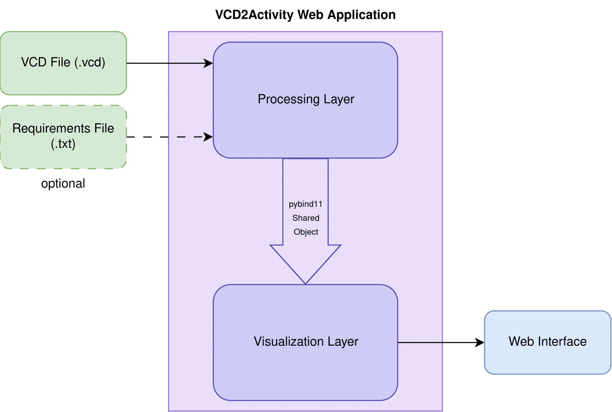
Fig 4. VCD2Activity web application architecture
Core Processing Layer & Data Structures
The processing layer is written in C++ and handles all the heavy lifting: parsing VCD files, reorganizing scope hierarchies, and evaluating compliance rules.
Written in C++, the parser reads the VCD file, reconstructs the design hierarchy and counts signal toggles using Hamming distance, so a 4-bit bus changing from 0101 to 1010 counts as 4 toggles, not 1. It also auto-detects the clock signal and groups timestamps into configurable sample windows. The parser uses a ToggleMap as the main data structure. It is an unordered map where each key is a scope name and each value is another unordered map of timestamps to toggle counts. This is later consumed by the other components of the processing layer and the visualization layer.
Scope Hierarchy Manipulation & Rule Compliance
Implemented also in C++, the merger lets engineers reorganize the scope hierarchy without re-running the simulation, supporting merge, rename, and remove operations. Because it operates directly on the hierarchy and toggle data in memory, engineers can restructure how signals are grouped. For example, combining repeated instances into a single logical block, normalizing naming across designs, or stripping out irrelevant test infrastructure. They can do this without paying the cost of re-simulating, which is an expensive step in the workflow.
The single-test checker evaluates user-defined compliance rules from a plain-text file, checking that per-scope toggle activity stays within percentage limits (PERCENTAGE rule) or compares correctly against each other (COMPARE rule), and returns pass or fail for each rule.
The wrapper compiles all of the above into a shared object binary using pybind11 [6], which Python imports at runtime with no manual data conversion needed.
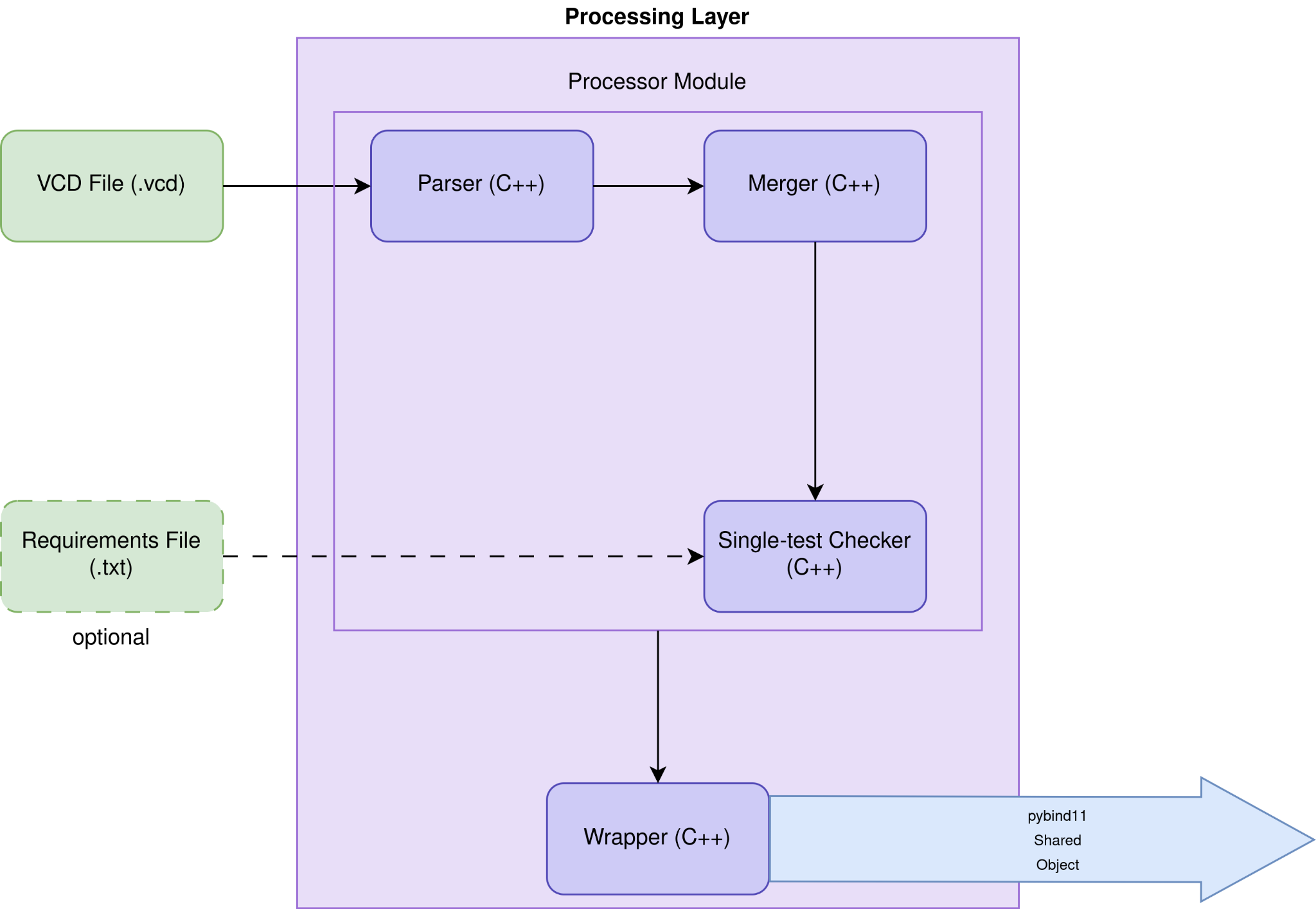
Fig 5. The processing layer architecture
Visualization Layer & Web Architecture
The visualization layer is written in Python and handles graph generation (via HoloViews [7], Matplotlib [8], and Bokeh [9]) and the web backend (via Flask [10]).
The plotter generates interactive trend graphs per scope and comparison charts across all scopes, with automatic activity window detection using K-Means clustering [11] and outlier detection using rolling IQR analysis.
Handling all server-side logic, the Flask backend manages sessions, caches results, and exposes everything through HTTP endpoints.
Built in plain HTML, CSS, and JavaScript, the frontend renders the scope tree, graphs, and compliance results in the browser without any client-side installation.
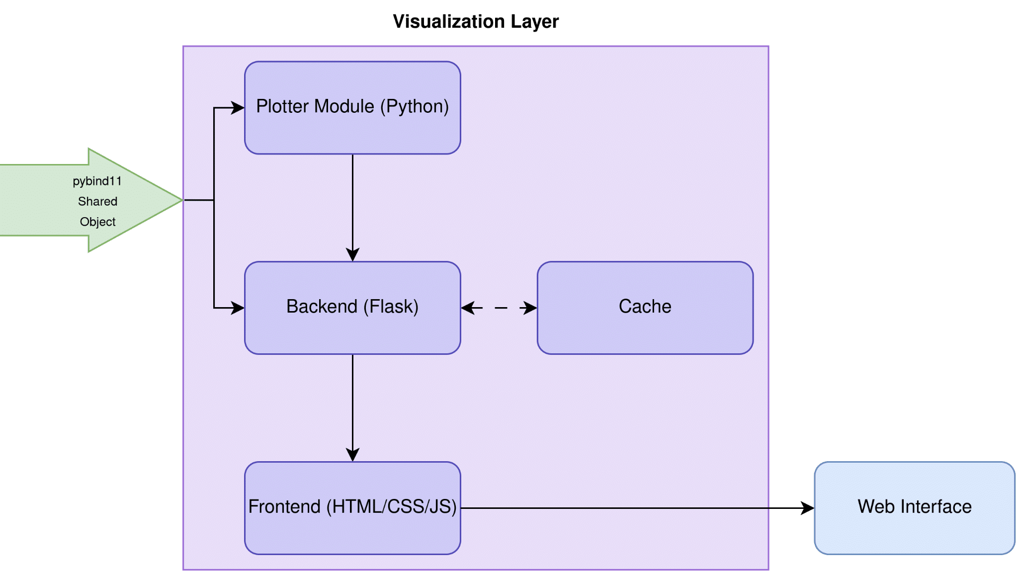
Fig 6. The visualization layer architecture
C++ Integration & Standalone Regression Automation
The bridge between them is pybind11, a header-only C++ library that compiles the C++ code into a shared object binary (.so) that Python can import at runtime like any other module. This means no manual data conversion: the C++ ToggleMap is automatically handed to Python as a native dictionary.
Separate from the web application, the regression checker is a standalone Python batch script that reuses the same C++ processing core. It takes a folder of VCD files and a requirements file as input, iterates through every test, and runs the parser and single-test checker on each one through the same wrapper. At the end it produces a HTML report summarizing the pass and fail results across all tests. Since it runs entirely from the command line and generates its own report, verification engineers can plug it directly into their post-simulation flow without ever opening a browser.
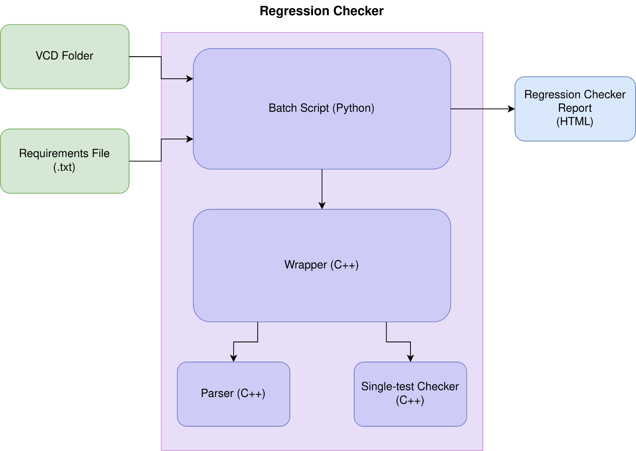
Fig 7. The regression checker architecture
6. Designs Used for Testing
The testing was carried out on real VCD files generated from three RTL designs, all simulated using the same simulator with a sample size of 100 ns.
The first design is a simple single-block square root unit. With only one scope and 17 signals, it represents the most straightforward case, a small, self-contained module with predictable toggle behavior.
A multi-module encryption subsystem containing 12 scopes and 106 signals is the second design. It contains five blocks which are connected serially.
The first block receives the serial input stream and extracts framing information. The serial data is then converted into a parallel bus for processing by the second block. The third block applies an encryption algorithm using an external key, and the data is handed off to the fourth block which converts it back to a serial stream. Finally, the last block applies a decryption algorithm, completing the encryption-decryption pipeline. The whole subsystem operates under a shared clock and reset interface, with status interfaces exposed on both the encryption and the decryption blocks.
This multi-module structure made this design the ideal candidate for validating the scope hierarchy, the merger, and the compliance checker. Each block has a distinct role and a different expected toggle profile, so checking whether their activity ratios are within defined limits is both meaningful and easy to verify.
The third design is a router with multiple configurable interfaces and routing logic. At 26 scopes and 341 signals it is the most complex of the three. It was used to validate that the tool handles designs with a large number of signals correctly and that the scope hierarchy, merger, and comparison charts scale to a realistic level of design complexity.
7. Results – Does It Actually Work?
The following graphs presented in this chapter come from testing the application on the encryption design. The blocks presented have the following format in the graphs, tb_top.subsystem.blockX, where X is the index of the block, from 1 to 5. Also there is a scope called tb_top.subsystem.local, with subsystem signals that are not from any of the blocks.
The single-test checker also was tested on the encryption design for one PERCENTAGE rule and three COMPARE rules and it presented this report to the user:
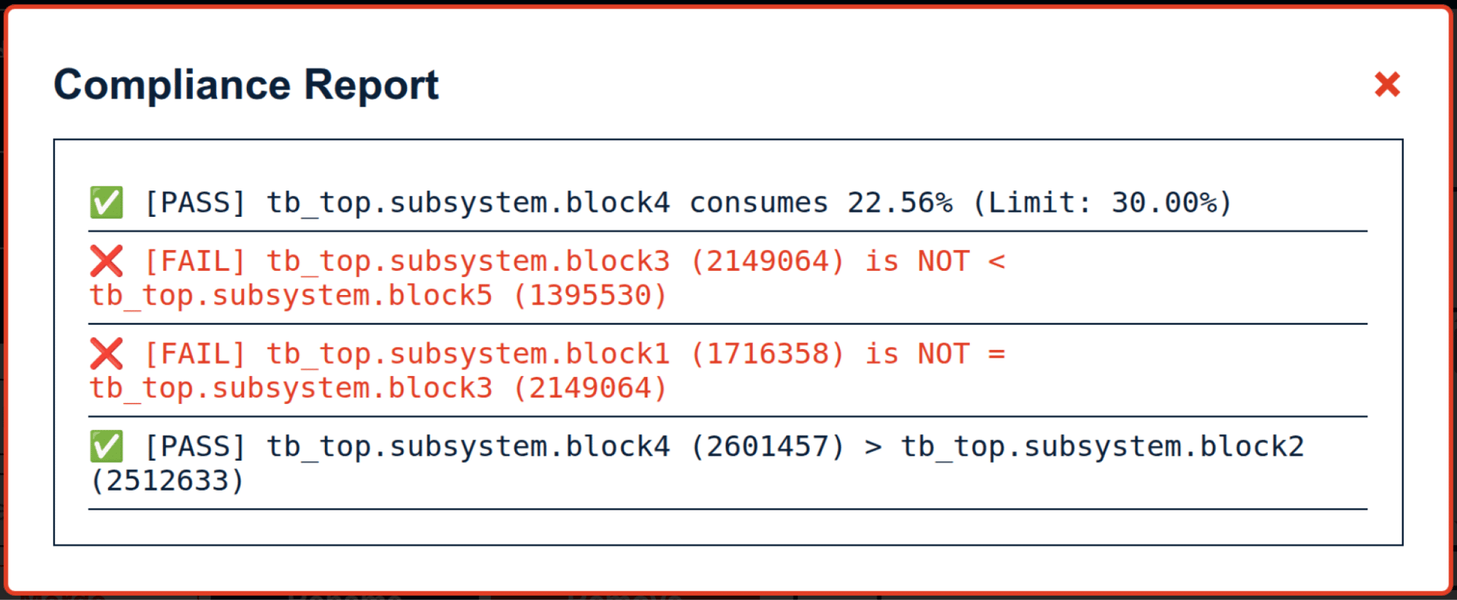
Fig 8. Single-test checker report for the encryption design
Simulation Timeline and Phase Detection
The trend graph for the top-level scope shows the full simulation timeline at a glance. Window 0 remains completely flat because the clock is gated and nothing toggles. During Window 1, a thin spike of minimal activity appears as the clock starts while the design is held in reset. Next, Window 2 shows low, sparse activity as the design comes out of reset with no traffic.
Things get interesting in Window 3, where toggle activity jumps sharply and stays high during the random traffic phase, with the color shifting from yellow to deep red to indicate increasing density. Window 4 represents the back-to-back peak throughput phase and forms visually the densest region of the graph. Finally, the last window shows activity dropping back down to a lower, irregular pattern matching the low-frequency traffic phase.
Magenta outlier dots correctly flag the highest individual spikes throughout the active windows, and the K-Means clustering correctly identifies and labels all six phases automatically without any manual input.
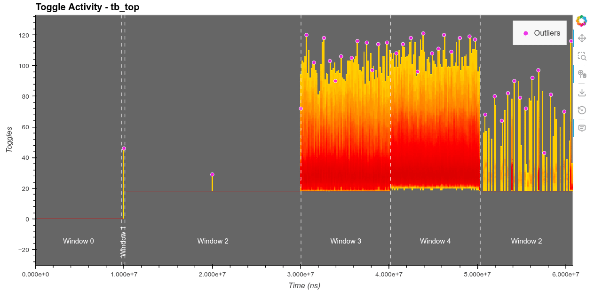
Fig 9. Toggle activity trend graph for the encryption design tb_top
Sub-Module Activity Ranking
Users can see the ranking of all the sub-modules by their total toggle count across the entire simulation with the bar chart. This immediately tells an engineer which blocks are the most active and therefore the largest contributors to toggle activity and, subsequently, to dynamic power. The fact that the parallel-to-serial and serial-to-parallel blocks are at the top makes intuitive sense, as they handle data conversion on every clock cycle. The encryption and decryption blocks operate on larger parallel chunks.
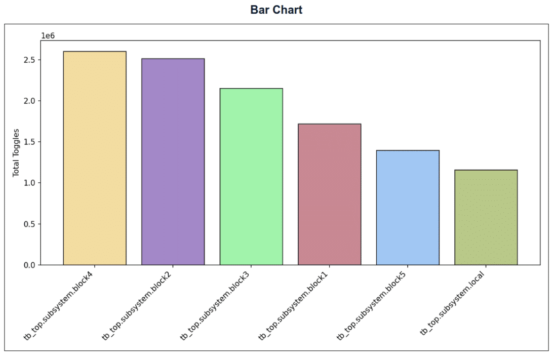
Fig 10. Toggle activity bar chart for the encryption design
Toggle Share Distribution
The pie chart expresses the same data as percentage shares of total toggle activity. This view is particularly useful for the single-test checker, because a PERCENTAGE rule like “block4 must not exceed 30% of total toggles” maps directly onto this chart. Here all modules are within a reasonable range of each other, suggesting a relatively balanced activity distribution across the pipeline.
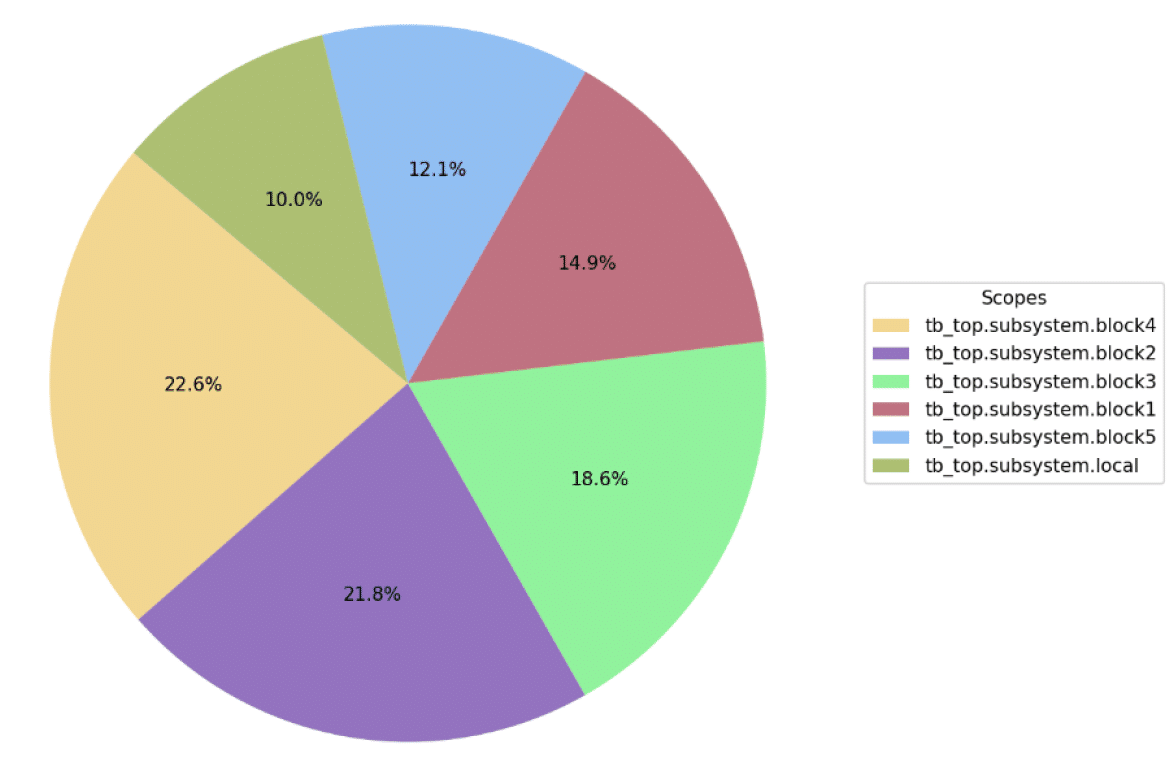
Fig 11. Toggle activity pie chart for the encryption design
Temporal Pipeline Flow & Stacked Activity
Each sub-module’s contributions to total activity over time are shown in the stacked area chart. What stands out here is that all modules scale up and down together in proportion. There is no single block dominating at one point while others are idle, which indicates the pipeline is flowing data through all stages simultaneously during active windows. The window boundaries are marked consistently with the trend graph, making it easy to cross-reference.
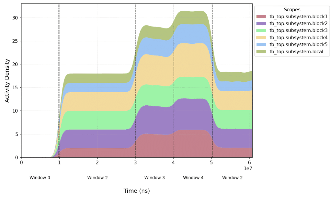
Fig 12. Toggle activity stacked area chart for the encryption design
Pipeline Heatmap & Hotspot Detection
The pipeline heatmap puts scopes on the Y axis and time on the X axis, with color intensity representing toggle density. The heatmap makes it immediately obvious which block at which point in time is the biggest power concern, which is exactly the kind of insight that would otherwise require manually inspecting individual waveforms.
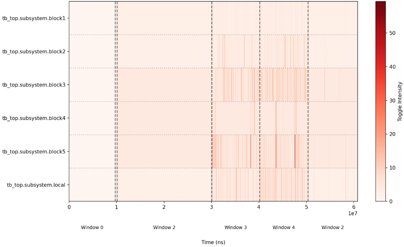
Fig 13. Toggle activity pipeline heatmap for the encryption design
Cumulative Energy Graph
Users can check the running total of toggles per scope over time with the cumulative energy graph. It is useful for understanding not just which block toggles the most in total, but how quickly that energy accumulates and how the designs behave in time. A block with a steep slope during peak traffic is a prime candidate for clock gating or other power optimization techniques.
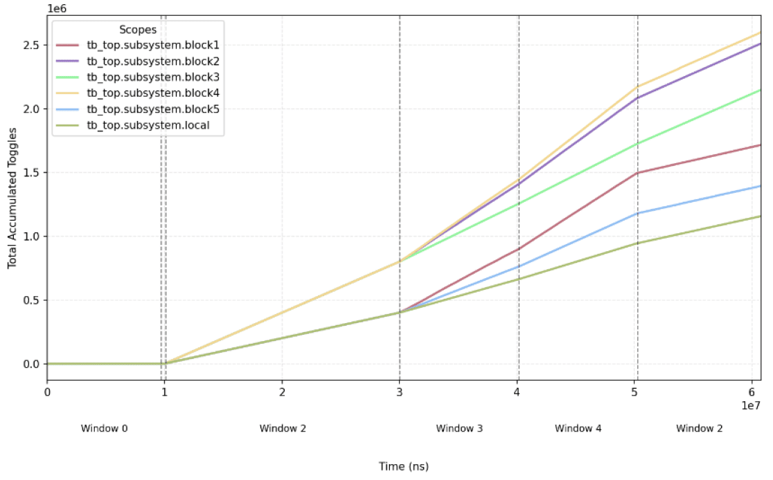
Fig 14. Toggle activity cumulative energy graph for the encryption design
Quantitative Metrics & Statistics Table
The statistics table consolidates the raw numbers behind all the charts. These numbers give engineers a precise, exportable summary of everything the graphs show visually.
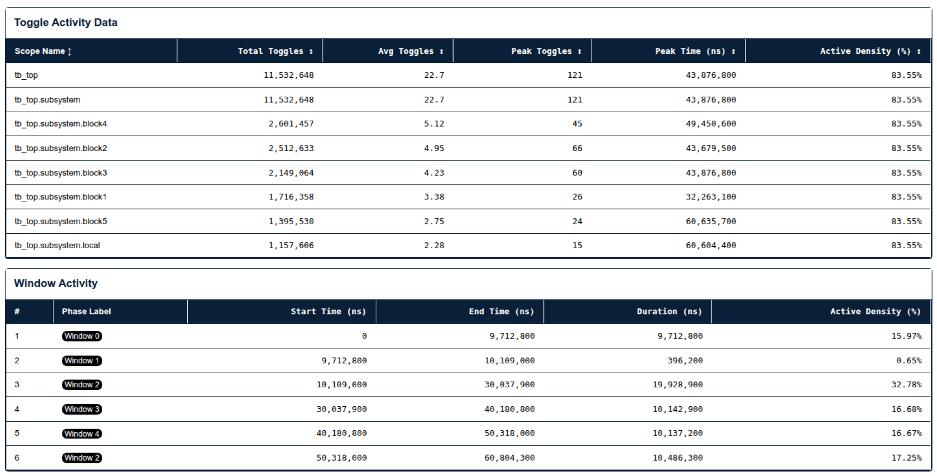
Fig 15. Toggle activity raw table statistics graph for the encryption design
Batch Regression Reporting & Rule Compliance
When it comes to the regression report, it shows the single-test checker running across 10 tests from the same regression folder. The fact that the same two rules fail identically across every single test is actually the most valuable output here: it tells the engineer that these are not random simulation artifacts but a structural characteristic of the design. That consistency is exactly what makes the regression checker useful, running it once across an entire batch immediately surfaces which compliance rules the design violates, saving the engineer from having to load each VCD individually.
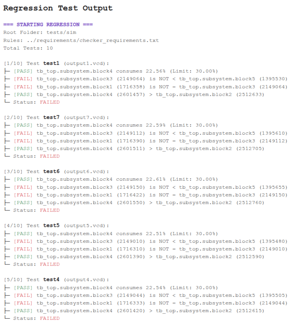
Fig 16. Snippet of regression checker HTML report with results for the first 5 out of 10 given tests
8. Performance – How Good Does It Work?
I tested VCD2Activity on the three RTL designs described in Chapter 5, all with the same 6 traffic windows:
- Window 1: Clock is gated, producing no toggle activity
- Window 2: Clock starts running but the design is held in reset
- Window 3: Reset is deasserted and the design becomes active with no traffic
- Window 4: Random traffic sequence begins
- Window 5: Back-to-back item sequence representing peak throughput
- Window 6: Low-frequency traffic with large inter-item delay
Also, all of the designs were simulated using 100,000 cycles for each window, so that the results were comparable:
Table 1: Performance measurements for the three designs on 100,000 window cycles
| Metric | VCD File 1 | VCD File 2 | VCD File 3 |
| File size | 19 MB | 67 MB | 46 MB |
| Active scopes | 1 | 26 | 12 |
| Number of signals | 17 | 341 | 106 |
| Parse time | 0.415s | 4.199s | 2.408s |
| Data transfer time (pybind11) | 0.115s | 1.989s | 1.268s |
| Total processing time | 0.530s | 6.188s | 3.676s |
| Size ratio | 1x | 3.53x | 2.42x |
| Parse time ratio | 1x | 10.12x | 5.80x |
| Total processing time ratio | 1x | 11.68x | 6.94x |
Parser Scalability & File Size Performance
For the encryption design, I also ran a scaling test to see how performance grows with file size, based on different window cycle values. The key finding: when design complexity is held constant, parse time scales linearly with file size. The biggest VCD file (2.3 GB, ~567 million toggles) took about 122 seconds to parse, exactly proportional to its size relative to the default 100,000 window cycles file for the encryption design.
Table 2: Encryption design performance measurements across increasing window cycle counts
| Metric | VCD File 3 | VCD File 4 | VCD File 5 | VCD File 6 | VCD File 7 | VCD File 8 |
| File size | 46 MB | 94 MB | 229 MB | 461 MB | 924 MB | 2.3 GB |
| Parse time | 2.408s | 3.992s | 9.799s | 21.167s | 42.040s | 121.965s |
| Data transfer time (pybind11) | 1.268s | 1.928s | 5.238s | 12.684s | 27.271s | 91.184s |
| Total processing time | 3.676s | 5.920s | 15.037s | 33.850s | 69.311s | 213.150s |
| Size ratio | 1x | 2.04x | 5.01x | 10.06x | 20.21x | 50x |
| Parse time ratio | 1x | 1.66x | 4.07x | 8.79x | 17.46x | 50.65x |
| Total processing time ratio | 1x | 1.61x | 4.09x | 9.21x | 18.85x | 58x |
The linear behavior I observed across different designs (the router took 10x longer to parse despite being only 3.5x larger than the square root design) was driven by signal count, not file size. More signals means more identifiers to resolve per timestamp. When you hold signal count constant, the parser is predictable.
8. Conclusions
VCD2Activity doesn’t replace gate-level signoff tools and it was never meant to. What it does is give engineers an early, practical window into signal toggling behavior at the RTL stage, right when fixing problems is still cheap: a few lines of code changed, not months of re-verification.
The main limitations are real and worth being honest about: toggle activity is an approximation of power, not a precise measurement. It presents information about hotspots and outliers of toggles so that the user can tell whether there are bugs or issues in the design. Very large files (multi-gigabyte range) can have long parse times. The K-Means window detection has fixed parameters that may not work perfectly on every design. These are all known tradeoffs of RTL analysis in general.
What the tool demonstrates is that meaningful RTL toggle analysis is possible with open-source technologies, no commercial license, no vendor lock-in, accessible from any browser, compatible with any simulator. For students, small teams, and engineers who want a quick power sanity check between simulation runs, VCD2Activity is a practical addition to the verification workflow.
Directions for future work: A multi-threaded parser for better performance on large files, time-windowed compliance rules (e.g., “check this scope only during window 3”), and potentially an AI layer that automatically flags anomalies and generates a natural language summary report without manual inspection.
9. Download
VCD2Activity’s source code can be found at AMIQ’s GitHub repository.