A key component of high-speed digital communication systems is clock recovery, which synchronizes the receiver's clock with the incoming data stream to allow for proper data interpretation. Phase-locked loops (PLLs) and other conventional techniques have difficulties in high-noise and ultra-low power settings, particularly when data rates are high. Shrinking transistors and rising bandwidth demands require more reliable clock recovery solutions.
We overcome these limitations in this study and present a bang-bang-like CDR implementation.
1. What is Clock Recovery?
In real-time systems, we cannot assume that the receiver and transmitter communicate at the same frequency. Each operates at its own internal clock speed, usually generated by a square wave oscillator (a 50-50 duty cycle signal). This creates a critical challenge: How can we guarantee the receiver captures exactly what the transmitter sent?
Digital signals have major analog restrictions when sent over long distances via physical medium like copper or fiber. These include reflections, noise, dispersion, and signal attenuation, all of which can skew or weaken the signal’s integrity. To maintain data integrity in high-speed serial transmissions over long distances, engineers must implement careful design, signal conditioning, and often deploy repeaters or equalizers.
Most digital systems use square waves as their clock reference, because they provide clear transitions between HIGH and LOW states. In an ideal scenario (Fig. 1), the transmitter (TX) and receiver (RX) would share a perfectly synchronized clock, ensuring error-free data sampling. In reality, though, this is rarely possible.
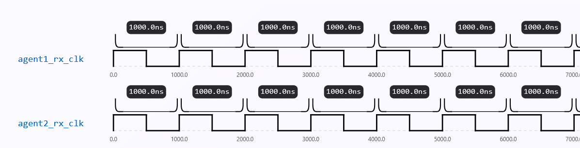
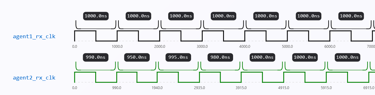
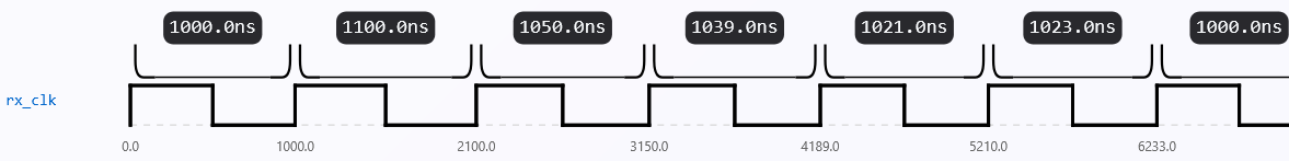
Even small frequency or phase differences result in sampling mistakes, which can corrupt data because TX and RX run on separate clocks (Fig. 2). This fundamental mismatch forces clock recovery systems to synchronize transmitter timing with receiver sampling.
2. The Consequences of Clocks Mismatch
Accurate clock recovery — the process by which a receiver aligns its internal clock with the incoming data stream from a transmitter — is essential to high-speed digital communication systems. Inaccuracies and possible system failure result from data sampling that is not properly aligned.
We cannot assume that the transmitter (TX) and receiver (RX) function at precisely the same frequency or phase in the majority of real-time systems. Usually, each makes use of an internal oscillator that produces a 50% duty cycle square wave signal. Although designed for clean HIGH/LOW transitions with sharp edges, these signals often exhibit phase and frequency mismatches.
Assuming perfect clock alignment with the TX, the RX should ideally sample incoming data exactly at the center of each bit period (Fig. 3).
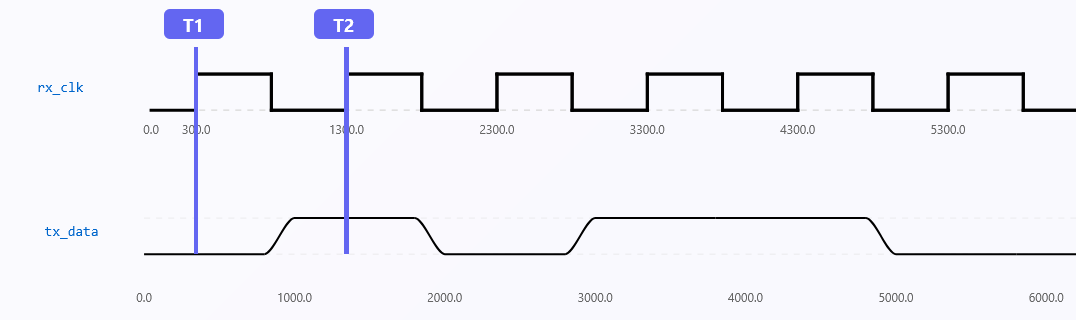
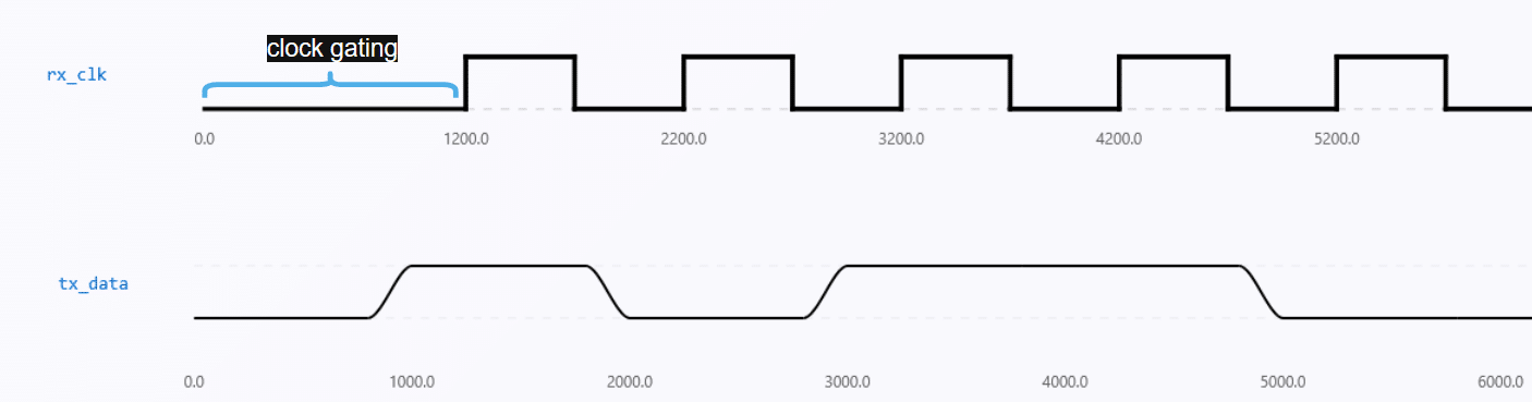
Data bits are accurately and neatly captured in this ideal situation. However, sampling misalignment occurs in real-world systems due to small differences in frequency (clock drift) or phase (timing offset) between TX and RX. This leads to data corruption, particularly when timing margins are small and data rates are high (Fig. 4). In the fourth figure, we’ve gated the clock to put into perspective erroneous sampling. The main source of the majority of clock recovery problems in real-world situations is persistent jitter, which is frequently brought on by EMI(electromagnetic interference). The clock recovery algorithm must therefore continuously check for and account for these phase fluctuations.
As system speeds rise and timing tolerance decreases, the effects of these mismatches worsen. As jitter builds up(Fig. 5) and bit errors increase in frequency, the receiver may finally misinterpret lengthy and constant bit sequences. Furthermore, conventional phase-locked loop (PLL)-based clock recovery methods have trouble maintaining synchronization in low-power or noisy situations, which are typical in contemporary mobile and Internet of Things applications. This is because of poor signal integrity and power limitations.
Clock recovery that is both dependable and effective is therefore crucial. The shortcomings of existing techniques under these difficult circumstances emphasize the necessity for innovative strategies. In this work, we offer a bang-bang-inspired clock and data recovery (CDR) architecture that operates under strict noise and power constraints, while tolerating larger clock discrepancies.
It is crucial to first examine the typical clock recovery methods now employed in digital communication systems in order to better comprehend the difficulties and direct the development of more reliable solutions.
3. Bang-Bang approach for Clock Data Recovery(CDR)
Over time, various techniques have been developed to achieve this synchronization, each with its own strengths and weaknesses depending on application requirements such as speed, power, and noise resilience. Below, we review the most common clock recovery methods. Among these, the Bang-Bang method has drawn the most attention because of its ease of use, dependability, and applicability for high-speed, low-power applications. In this article, we will be focusing on an approach inspired by the Bang-Bang CDR and its application, which tackles a number of issues that traditional clock recovery circuits encounter, especially in noisy and power-constrained settings.
3.1 Our Bang-Bang Inspired CDR Architecture
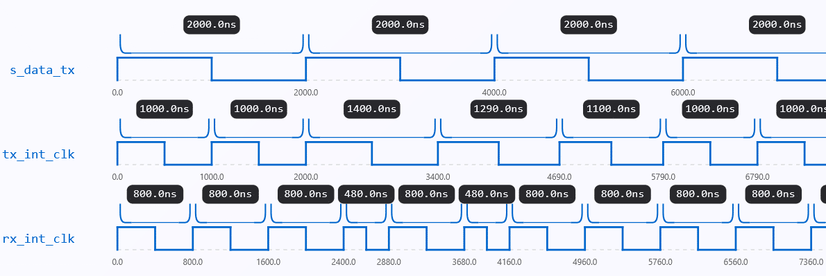
Before diving into the code, I’ll show a practical example of how clock recovery works. This mechanism ensures that the receiver clock is dynamically and incrementally adjusted during simulation whenever a significant timing mismatch is detected. Below(Fig. 6) is an example from the simulation environment that shows how the correcting process works:
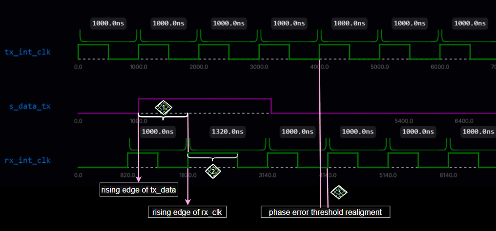
Note: The signal s_data_tx is essentially the same as s_data_rx with respect to rx_internal_clk. This is because the transmitter and receiver share the same data stream in this context—the data sent (tx) is the same data received (rx).
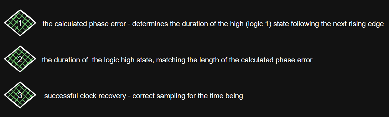
In the above diagram, a clock recovery example is illustrated with numbered diamonds. The explanations for each numbered diamond are provided below.
Mathematical Breakdown of Phase Error Computation
To compute the phase error, consider the following:
- The positive edge of
s_data_txoccurs at 1000 ns. - The first positive edge of the
rx_internal_clockthat follows this event occurs at 1820 ns.
Therefore, the phase error is calculated as: Phase error = 1820 ns − 1000 ns = 820 ns.
This 820 ns represents the duration of the positive edge of the recovered clock signal.
Assuming a symmetric square wave, the negative edge will follow after the clock’s initial half-period—500 ns in this example.
After applying this correction, the sampling aligns correctly: although the clocks remain out of phase, they are now synchronized in a way that ensures accurate sampling of the data stream.
3.1.1 Code Walkthrough: Bang-Bang CDR in Action
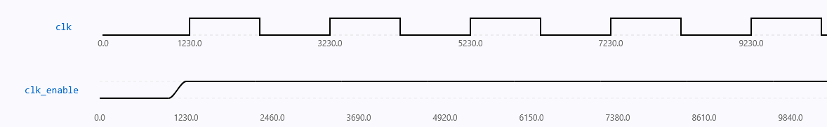
Let’s first clarify the environment in which this example takes place. Each of our two agents has an internal clock that runs at the same nominal time. Each agent’s clock_generator contains a clock_enable field to model real-world clock mismatch. During simulation, this field randomizes to gate the clock (Fig. 7) for random intervals, controlling when clock driving begins. In order to provide a realistic environment for clock recovery testing, this guarantees that the clocks begin out of phase and misaligned.
begin
      wait (cfg.clk_enable == 0);
      # (get_random_delay(1500, 2000)) cfg.clk_enable = 1;
end
The wait block is necessary to asynchronously wait for the clock enable signal to go low, since its initial value is unpredictable in simulation
In order to start appropriate clock recovery, this method ensures that the clocks are initially out of phase.
To measure the alignment between the data and the receiver’s internal clock, we implement a compute_phase_error task. This task, which keeps track of the phase difference between the internal clock and the incoming data, runs continuously throughout the simulation. A fork…join_none block is used to launch the task during run phase so that it can execute concurrently all of the remaining testbench operations.
This task runs permanently in the background, as it is launched in parallel as a standalone thread(as implied by join_none).
task compute_phase_error();
    forever begin
        @ (posedge vif.s_data_rx);
        last_edge_time = $time();

        @ (posedge vif.rx_internal_clk);
        phase_err = $time() - last_edge_time;
    end
endtask
The task operates by first sampling the timestamp of the incoming data edge (s_data_rx) and then waiting for the next rising edge of the receiver’s internal clock (rx_internal_clk). The time difference between these two edges is calculated and stored as phase_err, which represents the instantaneous phase error. This error measurement is crucial for driving the behavior of the Bang-Bang CDR mechanism.
As can be seen below, the task is only initiated during simulation when the internal clock is present:
if (`HAS_INTERNAL_CLK) begin
    fork
        compute_phase_error();
    join_none
end
If the `HAS_INTERNAL_CLK flag is not set, the simulation operates with a fixed external clock. In this configuration, both agents derive their clocks from the same source, meaning their clocks remain continuously aligned and in phase, meaning that there is no need for active clock recovery or phase error computation.
3.2 Phase Error Correction Mechanism
Once the phase_err is computed, the receiver must determine whether it falls outside an acceptable timing margin. Our implementation uses a predetermined threshold value (CLOCK_PHASE_ERROR_THRESHOLD) to carry out this check. To synchronize the receiver’s internal clock with the incoming data stream, the system starts a correction if the absolute phase error is greater than this threshold.
A dedicated correction process handles this procedure, running concurrently with all other transmitter (TX) and receiver (RX) clock driving processes.. The logic is as it follows:
- Threshold Detection: The recovery process waits until phase_err exceeds the threshold, indicating that the receiver is sampling too early or too late relative to the data edge.
- Clock Process Interruption: The current rx_clk_driving_p process is forcibly terminated using .kill(). This ensures we can override its behavior.
- Phase Correction via Logic High Extension: The internal clock is held high for an extended period equal to phase_err. This effectively shifts the clock phase forward by delaying the falling edge.
- Clock Realignment: After the delay, the clock is driven back to logic 0.
begin
      process recovery = process::self();

      // * Clock Recovery
      wait (phase_err > `CLOCK_PHASE_ERROR_THRESHOLD);

      // * Kill the clock driving process
      rx_clk_driving_p.kill();

      // * Extend the High State of the Clock by "phase_err"ns amount
      # (phase_err);

     // * Transition back to logic 0
     vif.rx_internal_clk <= 0;

     // * Reset the computed phase error to its default value
     phase_err = 0;
end
Clock recovery is an active and continuous process, it’s not done only once. This is checked every time a new phase error is being computed ensuring that the phase error threshold is not exceeded. Correct sampling at a single point in the simulation does not guarantee correct sampling throughout, as jitter and other timing variations can affect the CDR operation over time.
4. Simulating Clock Jitter
Clock jitter — tiny, unpredictable timing fluctuations in clock edges — is a key real-world defect that designers must simulate to fully evaluate our clock and data recovery(CDR) method’s resilience. At high rates, jitter can severely impact data sampling reliability
In our testbench, we add jitter only on the transmitter’s internal clock. The transmitter clock ties directly to the data stream (s_data_tx), making it the most realistic point to inject timing noise. Meanwhile, the receiver must recover a stable clock despite these irregularities — the core challenge of any CDR system.
The following code illustrates the application of jitter to the TX clock:
begin
     tx_clk_driving_p = process::self();
     forever # cfg.half_period begin : tx_internal_clk_driving
             // * Adding some clock drift
             if (cfg.has_clock_drift) begin
                  if (!std::randomize(clock_drift) with {
                      clock_drift inside {[0 : cfg.half_period * `CLOCK_JITTER_PERCENTAGE]};
                  })
                     `uvm_fatal(get_full_name(), "Couldn't randomize CLOCK_DRIFT")

                     # clock_drift;
              end

               vif.tx_internal_clk <= !vif.tx_internal_clk;
     end
end
In our simulation, we limit the maximum clock jitter to 20% of the half clock period using the constraint from above.
In real high-speed communication systems, jitter above about 20% of the clock period(Fig. 8) usually causes serious problems for accurate data sampling. When jitter gets too large, the clock edges can shift too close to the data transitions, which leads to more sampling errors, corrupted bits, and potentially a complete failure to recover the data.
We replicate difficult but yet controllable situations for our clock recovery algorithm by capping jitter within this range. Meaningful data recovery would be impossible if jitter were permitted to go beyond this threshold since the receiver would find it difficult, if not impossible, to properly align its clock.